400-6505-735

News
CIF focuses on material surface treatment technology, providing customers with professional instrument equipment and application process solutions for cleaning, debonding, etching, coating and other aspects!With the continuous development of semiconductor technology, the requirements for process technology are getting higher and higher, especially the surface quality requirements for semiconductor wafers are getting stricter and stricter. The main reason is that the particles and metal impurities on the surface of the wafer will seriously affect the quality and yield of the device. In the current integrated circuit production, more than 50% of the material is still lost due to the surface contamination of the wafer.
In the semiconductor production process, cleaning is required in almost every process, and the quality of wafer cleaning has a serious impact on the performance of the device. It is precisely because wafer cleaning is the most important and frequent step in the semiconductor manufacturing process, and its process quality will directly affect the yield, performance and reliability of the device, so major companies and research institutions at home and abroad have been continuously conducting research on cleaning processes. Plasma cleaning machine, as an advanced dry cleaning technology, has the characteristics of green environmental protection. With the rapid development of the microelectronics industry, plasma cleaning machine is also increasingly used in the semiconductor industry.
Contamination impurities and classification of semiconductors
Semiconductor manufacturing requires the participation of some organic and inorganic substances. In addition, since the process is always carried out in a clean room with the participation of people, semiconductor wafers are inevitably contaminated by various impurities. According to the source and properties of pollutants, they can be roughly divided into four categories: particles, organic matter, metal ions and oxides.
1.1 Particles
Particles are mainly some polymers, photoresists and etching impurities. This type of pollutant usually relies on van der Waals attraction to adsorb on the surface of the wafer, affecting the formation of geometric figures and electrical parameters of the device photolithography process. The removal method of this type of pollutant is mainly to undercut the particles by physical or chemical methods, gradually reduce the contact area between the particles and the wafer surface, and finally remove them.
1.2 Organic matter
The sources of organic impurities are relatively wide, such as human skin oil, bacteria, machine oil, vacuum grease, photoresist, cleaning solvents, etc. This type of pollutant usually forms an organic film on the surface of the wafer to prevent the cleaning liquid from reaching the surface of the wafer, resulting in incomplete cleaning of the wafer surface, so that pollutants such as metal impurities remain intact on the surface of the wafer after cleaning. The removal of this type of pollutant is often carried out in the first step of the cleaning process, mainly using methods such as sulfuric acid and hydrogen peroxide.
1.3 Metals
Common metal impurities in semiconductor processes include iron, copper, aluminum, chromium, tungsten, titanium, sodium, potassium, lithium, etc. The sources of these impurities are mainly: various utensils, pipes, chemical reagents, and various metal contaminations generated during the formation of metal interconnections during the processing of semiconductor wafers. The removal of such impurities is often carried out by chemical methods. The cleaning solution prepared by various reagents and chemicals reacts with metal ions to form a complex of metal ions and detach from the surface of the wafer.
1.4 Oxides
When semiconductor wafers are exposed to an environment containing oxygen and water, a natural oxide layer will form on the surface. This oxide film not only hinders many steps in semiconductor manufacturing, but also contains certain metal impurities. Under certain conditions, they will be transferred to the wafer to form electrical defects. The removal of this oxide film is often completed by soaking in dilute hydrofluoric acid.
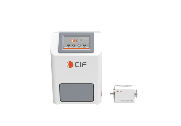
Application of plasma cleaning machine in semiconductor wafer cleaning process Plasma cleaning has the advantages of simple process, convenient operation, no waste disposal and environmental pollution. However, it cannot remove carbon and other non-volatile metal or metal oxide impurities. Plasma cleaning is commonly used in the process of removing photoresist. A small amount of oxygen is introduced into the plasma reaction system. Under the action of a strong electric field, the oxygen generates plasma, which quickly oxidizes the photoresist into a volatile gas state substance that is pumped away. This cleaning technology has the advantages of easy operation, high efficiency, clean surface, no scratches, and is conducive to ensuring product quality in the photoresist removal process. Moreover, it does not require acid, alkali, and organic solvents, so it is increasingly valued by people.
About Us
Introduction Culture History HonorNews
News Article VideoService
After-sale ServiceNavigation
ProductsSolutionContact Us 400-6505-735
 CIF WeChat Service Account
 CIF Tiktok

 2024-09-06
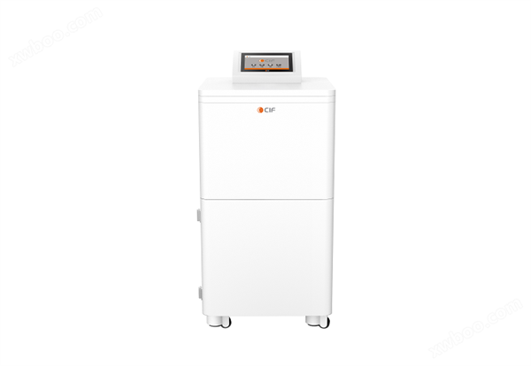
 Add WeChat