400-6505-735

The current domestic IC packaging process is mainly divided into front-end, middle-end and back-end processes. Only products with good packaging quality can become terminal products and thus be put into practical application in the industry.
The front-end process steps are:
1) Chip mounting: Use protective film and metal frame to fix the silicon wafer;
2) Slicing: Cut the silicon wafer into individual chips and test the chips to screen the qualified chips;
3) Chip mounting: Apply silver glue or insulating glue to the corresponding position of the lead frame, remove the cut chip from the slicing film, and bond the chip to the fixed position of the lead frame;
4) Bonding: Use gold wire to connect the lead holes on the chip and the pins on the frame to connect the chip to the external circuit;
5) Plastic encapsulation: Plastic encapsulate the circuit of the components to protect the components from external damage and strengthen the physical properties of the components;
6) Post-curing: Curing the plastic encapsulation material to make it have sufficient strength to meet the entire packaging process.
The lead frame is the carrier of the chip. It is an important structural part that uses bonding wires to connect the lead end of the chip's internal circuit to the external lead to form an electrical circuit, and plays a bridge role in connecting with external wires. The lead frame is used in many semiconductor integrated blocks and is an important basic material in the semiconductor industry. The IC packaging industry process must be completed on the lead frame. The pollutants present in the packaging process are an important factor restricting its development.
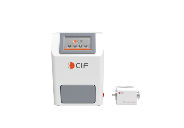
The plasma cleaning process is the only dry cleaning method without any environmental pollution. The plasma action under vacuum can basically remove inorganic/organic pollution on the surface of the material, improve the surface activity of the material, increase the bonding ability of the lead, and prevent the delamination of the package.
The application of plasma cleaning technology in the IC packaging industry is mainly in the following aspects:
1) Before dispensing If there are contaminants on the workpiece, the silver glue on the workpiece will form a spherical shape, which greatly reduces the adhesion with the chip. Plasma cleaning can increase the hydrophilicity of the workpiece surface, improve the success rate of dispensing, and save the amount of silver glue used, reducing production costs.
2) Before wire bonding After the packaged chip is pasted on the lead frame workpiece, it must be cured at high temperature. If there are contaminants on the workpiece, these contaminants will cause poor welding effect or poor adhesion between the lead and the chip and the workpiece, affecting the bonding strength of the workpiece. The plasma cleaning process is used before wire bonding, which will significantly increase its surface activity, thereby improving the bonding strength of the workpiece and the uniformity of the tension of the bonding wire.
About Us
Introduction Culture History HonorNews
News Article VideoService
After-sale ServiceNavigation
ProductsSolutionContact Us 400-6505-735
 CIF WeChat Service Account
 CIF Tiktok

 2024-09-06
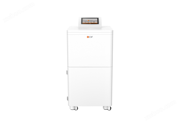
 Add WeChat